Quantum Dot Supernova-like-Shaped Arsenic (III) Sulfide-Oxide/Polypyrrole Thin Film for Optoelectronic Applications in a Wide Optical Range from Ultraviolet to Infrared
A quantum dot (QD) thin film of arsenic (III) oxide-hydroxide/polypyrrole (As2S3-As2O3/Ppy) with a supernova-like shape has been developed for optoelectronic applications across a wide optical range, spanning from ultraviolet (UV) to infrared (IR). The fabrication process involves the polymerization of pyrrole to form Ppy in the presence of NaAsO2 and K2S2O8. The resulting QD exhibits a remarkable morphology characterized by a supernova-like structure and a porous nature with a particle size of 4 nm. The unique morphology of the QD contributes to its optical properties. The material demonstrates a maximum optical absorbance that extends up to 600 nm. The chemical structure of the composite has been proved using various characterization techniques. The As2S3-As2O3/Ppy QD thin film holds significant potential for optoelectronic applications, particularly in light detection across multiple optical regions. Its sensitivity has been evaluated through the measurement of photoresponsivity (R), yielding a high value of 0.31 mA/W. This indicates a substantial current density (Jph) of 0.031 mA/cm2 at a wavelength of 340 nm. Additionally, the detectivity (D) of the photodetector has been calculated based on these values, resulting in a detection capability of 6.9 × 10⁷ Jones. This indicates the ability to detect low levels of photons using this photodetector. The highly reproducible nature of this photodetector enables its application in various optoelectronic systems. The As2S3-As2O3/Ppy QD thin film offers great promise as a versatile optoelectronic application with its wide optical range, excellent sensitivity, and detectivity. Researchers have successfully developed photodetector applications that have been extended to cover several domains including lighting, smart windows, and spacecrafts. They are exploring the possibility of combining polymers with nanomaterials possessing beneficial optical properties to improve optical performance in optoelectronic devices. The study of controlling the morphology of polymer composites holds great promise for advancing optical applications, and the development of these composites opens up possibilities for advancements in solar cells, light-emitting diodes (LEDs), photodetsors, and other optoelecticronic devices, as well as other studies using other composites with small J values. To solve this issue, researchers have tried to modify the active sites by changing the shape, shape, and nanodetectors, but this research has failed.
Publicerad : 3 år sedan förbi Ben Gouider Trabelsi, Amira, M. Elsayed, Asmaa, Fatemah, H. Alkallas, Mohamed, Rabia i Science
signature of the photoelectrochemical process rate. Optoelectronic devices, particularly photodetectors, have experienced fast progress within the last decade. Photodetector applications have been extended to cover several domains including lighting, smart windows, and spacecrafts [ 1 2 ]. This is owing to their excellent photo response to different illuminations associated with the produced Jsignature of the photoelectrochemical process rate. Polymers possess advantageous optical properties that can be further improved through the creation of composites with nanomaterials possessing beneficial optical properties. By controlling the morphology of these composites, their optical characteristics can be enhanced. Incorporating small particles into the composite structure adds additional optical properties, expanding their potential in optoelectronic systems. 4, Combining polymers with nanomaterials having enhanced optical properties leads to synergistic effects, resulting in unique functionalities and improved performance in optoelectronic devices. The small size of nanoparticles contributes to their exceptional optical properties, such as enhanced light absorption, emission, or scattering. These properties can be precisely adjusted by manipulating the size, shape, and composition of the nanoparticles, enabling precise control over the optical behavior of the composite material. The use of these nanocomposites in optoelectronic systems holds significant potential, finding applications in photovoltaics, light-emitting devices, sensors, optical filters, and displays. The insertion of inorganics into polymers increases their optical properties but also imparts additional functionalities, such as improved charge transport, increased stability, or enhanced mechanical properties [ 3 5 ]. Overall, the formation of composites by combining polymers with nanomaterials possessing high optical properties, alongside morphological control, opens up new avenues in optoelectronic systems. Harnessing the unique optical characteristics of small particles in these composites paves the way for advanced applications and advancements in the field of optoelectronics [ 6 ]. The study of controlling the morphology of polymer composites holds great promise for advancing optical applications. Researchers are particularly interested in synthesizing composites with a 2D structure or incorporating quantum dots to achieve desired properties. These approaches offer exciting possibilities for enhancing the optical performance of the materials. When a polymer composite is confined to a 2D thin film structure, it exhibits additional behaviors that are not present in bulk materials. This includes improved atom ordering and novel optical properties. The 2D nature of the composite enables precise control over its structure and properties, allowing for tailored optical behavior. The combination of inorganic materials and polymers in a 2D composite introduces new features that make them highly recommended for applications in advanced devices. These materials demonstrate unique characteristics, such as enhanced light absorption, efficient charge transport, and improved optoelectronic performance. These properties make them particularly well suited for applications in fields like photovoltaics and optoelectronics. The integration of 2D inorganic-polymer composites into highly technological devices offers several advantages. Their optimized morphology and structure result in improved device performance and efficiency. Furthermore, the compatibility of these composites with existing manufacturing processes and cost-effective synthesis methods makes them attractive options for commercial applications. 8, The development of such composites opens up possibilities for advancements in solar cells, light-emitting diodes (LEDs), photodetectors, and other optoelectronic devices. Researchers are actively exploring these materials to harness their full potential and contributions to the advancement of high-tech applications [ 7 9 ]. By utilizing the unique properties of 2D thin film composites and quantum dot incorporation, scientists aim to unlock new opportunities for highly efficient and versatile photovoltaic and optoelectronic devices. Continued research and development in this area holds significant potential for driving innovation and pushing the boundaries of technological advancements in the field [ 10 ]. = 20 µA). Similarly, other studies using other composites and polymers demonstrate small J values (107 µA) [ values remain low. Furthermore, some polymers’ photodetector synthesis could be costly compared to their low reproducibility, i.e., low R or D values detected in a single spectral domain (UV, Vis, or near IR). This approach combines polymers with inorganic materials to improve their photo detectivity [13,14, Prior studies have utilized metal-based materials for photodetector development. Nevertheless, such a photodetector remains unable to detect light within a broad spectral domain. To solve this issue, researchers have tried to modify the active sites by changing the material shape, i.e., nanorods, nanotubes, nanowires, and nanosheets. Several studies have succeeded so far in partially solving this impediment. Wang et al. [ 11 ] developed a CuO nanowire photodetector for the IR domain, but it had a weak response (J= 20 µA). Similarly, other studies using other composites and polymers demonstrate small Jvalues (107 µA) [ 12 ]. In this regard, researchers have investigated conductive polymers like poly-3-hexylthiophene. Nevertheless, the obtained Jvalues remain low. Furthermore, some polymers’ photodetector synthesis could be costly compared to their low reproducibility, i.e., low R or D values detected in a single spectral domain (UV, Vis, or near IR). This approach combines polymers with inorganic materials to improve their photo detectivity [ 10 15 ]. Herein, a quantum dot was synthesized by combining Ppy with porous spherical As O -As(OH) , using NaAsO . The resulting QD exhibited a highly porous structure, which is beneficial for light detection applications. It demonstrated excellent light detection capabilities across a wide range of light frequencies, spanning from UV to IR. The composite exhibited high responsivity and detectivity values, indicating its sensitivity and efficiency in converting incident light into an electrical signal.
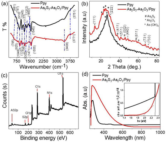
S -As O /Ppy QD was analyzed by examining the main functional groups through FTIR analysis, as shown in S -As O /Ppy are provided in S -As O -As(OH) has a limited effect on electron vibration. However, slight shifts in certain functional groups can be observed [17,−1 to 3754 cm−1 after the composite formation, indicating a slight blue shift. Similarly, the C=C benzene group also exhibits a blue shift. On the other hand, the C=C quinoid group shows a red shift after composite formation. The chemical composition of the As-As/Ppy QD was analyzed by examining the main functional groups through FTIR analysis, as shown in Figure 1 a. The locations of the functional groups in Ppy and As-As/Ppy are provided in Table 1 . The functional groups in pure Ppy and the QD have the same positions. The main functional groups in both the pure polymer and the composite exhibit similar locations, indicating that the incorporation of As-As-As(OH)has a limited effect on electron vibration. However, slight shifts in certain functional groups can be observed [ 16 18 ]. For example, the N-H group shows a shift from 3771 cmto 3754 cmafter the composite formation, indicating a slight blue shift. Similarly, the C=C benzene group also exhibits a blue shift. On the other hand, the C=C quinoid group shows a red shift after composite formation. S -As O /Ppy QD was confirmed through XRD analysis, as depicted in O nanomaterial was evidenced by the peaks observed [ S materials. Additionally, the peaks at 48.9° and 59.9° indicate the presence of As(OH) inorganic material [ The chemical crystalline behavior of Ppy and the As-As/Ppy QD was confirmed through XRD analysis, as depicted in Figure 1 b. The presence of Asnanomaterial was evidenced by the peaks observed [ 21 ] at 13.4°, 29.8°, 41.4°, 45.7°, 67.7°, and 70.9°, corresponding to the crystallographic planes (111), (222), (511), (440), (731), and (733), respectively. The three characteristic peaks at 37.5° (411), 46.1° (002), and 57.6° (611) clearly represent the Asmaterials. Additionally, the peaks at 48.9° and 59.9° indicate the presence of As(OH)inorganic material [ 22 ]. With the incorporation of these inorganic materials inside the polymer matrix, the shape of the peaks show loss of intensity from the coating with the organic material. The polymer Ppy exhibited peaks in the range of 21.4° to 27.6°, with four characteristic peaks observed within the QD. However, in pure Ppy, only two peaks were observed, located at 24.6° and 27.4°. S -As O /Ppy QD play a crucial role in its potential application as a photoelectrode for photocatalytic purposes. The absorbance behavior of this QD is depicted in O -As(OH) into the Ppy matrix has a synergistic effect, enhancing the optical absorbance of the QD. The absorbance properties of the As-As/Ppy QD play a crucial role in its potential application as a photoelectrode for photocatalytic purposes. The absorbance behavior of this QD is depicted in Figure 1 d, where it shows a wide absorbance range that extends up to 610 nm, indicating its excellent ability to absorb photons. In contrast, the pure Ppy material exhibits absorbance mainly up to the beginning of the visible region. This suggests that the incorporation of As-As(OH)into the Ppy matrix has a synergistic effect, enhancing the optical absorbance of the QD. S -As O /Ppy QD were calculated. The QD exhibits a promising bandgap energy of 1.95 eV, determined using the Tauc equation (Equation (1)) [ ). This bandgap value underscores the potential of the QD for efficient light absorption and utilization in photocatalytic applications. To further support this observation, the bandgap energies of both pure Ppy and the As-As/Ppy QD were calculated. The QD exhibits a promising bandgap energy of 1.95 eV, determined using the Tauc equation (Equation (1)) [ 23 24 ] and considering the absorbance coefficient (). This bandgap value underscores the potential of the QD for efficient light absorption and utilization in photocatalytic applications. The narrow bandgap of As S -As O /Ppy materials demonstrates their high applicability in optoelectronic systems. This characteristic makes them sensitive to photons with different frequencies and energies. The promising conditions arising from this narrow bandgap suggest that these materials are well suited for use in various optoelectronic devices, particularly in light-sensing applications across a wide range of wavelengths. Due to the small bandgap, the As S -As O /Ppy materials can efficiently absorb photons with diverse energies, allowing them to detect light signals across a broad spectrum. This versatility in light absorption is a significant advantage for optoelectronic devices, as it enables them to be highly responsive to different wavelengths of light. The sensitivity of these materials to various frequencies and energies of photons opens up opportunities for their application in a wide range of optoelectronic systems. Whether visible light, ultraviolet, or infrared radiation, the As S -As O /Ppy materials have the potential to fulfill light sensing requirements under different wavelength conditions. So, the small bandgap of As S -As O /Ppy materials indicates their high applicability in optoelectronic systems. Their sensitivity to photons with different frequencies and energies enables efficient light absorption across a broad spectrum, making them well suited for various optoelectronic devices, especially in light sensing applications under diverse wavelength conditions. This adaptability and versatility pave the way for potential advancements in optoelectronics and their integration into a wide array of technological applications. S -As O /Ppy film elemental analyses were proved through XPS ( As-As/Ppy film elemental analyses were proved through XPS ( Figure 1 c). The XPS survey spectrum revealed the arsenic (As) and oxygen (O) in the composite material. The As 3d peak was observed at an energy of 42 eV, confirming the presence of arsenic in the composite. Furthermore, a significant amount of oxygen was detected, as indicated by the O1s peak at approximately 532 eV. This observation suggests the formation of As O -As(OH) filler material within the polymer matrix. Moreover, the peak of the S element was confirmed at 164 eV, related to the As S nanomaterial. It can be inferred that the polymer coats this filler material, resulting in the composite structure. The carbon (C) atom formation of benzene or quinone C=C bonds within the Ppy ring structure was confirmed. The presence of nitrogen (N) was also identified, indicating the presence of the polymer material. In summary, XPS measurements confirmed the presence of arsenic and oxygen in the As S -As O /Ppy films. The XPS survey spectrum revealed the formation of As2S3-As O with traces of As(OH) filler material embedded within the polymer matrix. The analysis also identified carbon and nitrogen atoms associated with the polymer component. These findings provide valuable insights into the elemental composition and structure of the composite material. S -As O /Ppy QD exhibits a supernova-like or star-like morphology, as depicted in Under SEM analysis, the As-As/Ppy QD exhibits a supernova-like or star-like morphology, as depicted in Figure 2 a,b. The polymer matrix acts as a cloud, while the inorganic particles are embedded within this cloud, creating a highly interconnected structure. This topography enhances the electrical and optical behavior of the QD. In contrast, the SEM image in Figure 2 c reveals a different morphological behavior for Ppy, where it appears as large particles separated from each other. Each of these particles consists of small, wrinkled particles that are combined to form the larger structure. Further confirmation of the supernova-like morphology is provided by the TEM image in Figure 2 d, which clearly shows the embedded inorganic materials within the polymer matrix. The theoretical modeling in Figure 2 e,f reinforces this morphology, with Ppy particles composed of numerous interconnected small particles, and the supernova-like shape illustrating the embedding of small inorganic particles within the polymer matrix. This morphology is highly desirable in various applications, such as photovoltaics, catalysis, and sensors, as it offers a large surface area for interactions with other materials and exhibits unique geometric properties that can enhance overall performance. The electrical performance of the As S -As O /Ppy QD photodetector involves analyzing its performance by studying its current–voltage characteristics under different light conditions. These measurements provide valuable insights into the device’s functionality, sensitivity, and overall performance. By examining the current–voltage (I–V) curve, important electrical parameters such as conductivity, resistance, and light response can be determined. Additionally, the I–V curve enables the evaluation of the dark J , which represents the current flowing in the absence of light, as well as the photocurrent (J ), which represents the current generated when light is incident on the device. S -As O /Ppy QD photodetector. To control the incident light wavelengths, optical filters were utilized. The unique composition of the QD, consisting of both organic and inorganic materials, enables the enhancement of optical absorbance across multiple regions, as indicated in the optical absorbance analysis ( and signifies the device’s sensitivity to incident photons within these specific regions. The estimation of these values was performed using an electrochemical CHI608E instrument, which allows for precise measurements of the electrical properties of the As-As/Ppy QD photodetector. To control the incident light wavelengths, optical filters were utilized. The unique composition of the QD, consisting of both organic and inorganic materials, enables the enhancement of optical absorbance across multiple regions, as indicated in the optical absorbance analysis ( Figure 1 d). Consequently, photons with UV or visible spectra wavelengths possess the ability to excite electrons, causing them to transition to the conducting band. This excitation produced Jand signifies the device’s sensitivity to incident photons within these specific regions. S -As O /Ppy QD photodetector, from −2 to +2 volts, is relatively small compared to the larger applied potentials used in previous studies, such as −5 to +5 V [ The potential range used in the electrical measurements of the As-As/Ppy QD photodetector, from −2 to +2 volts, is relatively small compared to the larger applied potentials used in previous studies, such as −5 to +5 V [ 25 ] or −7 to +7 V [ 26 ]. This indicates that the QD has a high sensitivity to the generation of hot electrons even under small-applied potentials. In other words, the device is capable of generating photocurrent and detecting light even with a relatively low voltage range, highlighting its efficiency and sensitivity as a photodetector material [ 27 28 ]. a demonstrates the behavior of the As S -As O /Ppy QD photodetector, as reflected in the values of J and J , which are measured at 0.052 and 0.02 mA/cm², respectively. The significant increase in the current values indicates the enhanced generation of hot electrons in response to light illumination. This suggests that the QD exhibits a heightened sensitivity to incident photons, resulting in a higher production of photocurrent compared to dark current. With the normal conductivity of semiconductor materials taken into consideration, the J value is considered a very small value and represents the effect of noise on this optoelectronic device [30,31, a demonstrates the behavior of the As-As/Ppy QD photodetector, as reflected in the values of Jand J, which are measured at 0.052 and 0.02 mA/cm², respectively. The significant increase in the current values indicates the enhanced generation of hot electrons in response to light illumination. This suggests that the QD exhibits a heightened sensitivity to incident photons, resulting in a higher production of photocurrent compared to dark current. With the normal conductivity of semiconductor materials taken into consideration, the Jvalue is considered a very small value and represents the effect of noise on this optoelectronic device [ Figure 3 a demonstrates the behavior of the As-As/Ppy QD photodetector, as reflected in the values of Jand J, which are measured at 0.052 and 0.02 mA/cm², respectively. The significant increase in the current values indicates the enhanced generation of hot electrons in response to light illumination. This suggests that the QD exhibits a heightened sensitivity to incident photons, resulting in a higher production of photocurrent compared to dark current. With the normal conductivity of semiconductor materials taken into consideration, the Jvalue is considered a very small value and represents the effect of noise on this optoelectronic device [ 29 32 ]. S -As O /Ppy QD under light is estimated through light controlling, as shown in −2, respectively. The on/off behavior of the As-As/Ppy QD under light is estimated through light controlling, as shown in Figure 3 b. To assess the reproducibility of the on/off light behavior, the experiments involved exposing the device to a controlled light source and measuring its response over several cycles of light exposure. By analyzing the recorded signals, the device’s capacity to consistently and accurately transition between the on and off states can be evaluated as indicated in Figure 3 b, in which the on/off values are 0.1 and 0.03 µA·cm, respectively. S -As O /Ppy QD is effectively controlled by manipulating the frequency and energy of incident photons using optical filters ( values of 0.031, 0.027, and 0.026 mA·cm−2 were obtained under optical filters with wavelengths of 340, 540, and 730 nm, respectively. values in a columnar format at a voltage of 2.0 V. The behavior of the As-As/Ppy QD is effectively controlled by manipulating the frequency and energy of incident photons using optical filters ( Figure 4 a). This control allows for precise modulation of sensitivity and controlled generation of hot electrons. The impact of optical filters is evident in the observed changes in Jph values under different conditions. Jvalues of 0.031, 0.027, and 0.026 mA·cmwere obtained under optical filters with wavelengths of 340, 540, and 730 nm, respectively. Figure 4 b provides a visual representation of the Jvalues in a columnar format at a voltage of 2.0 V. −19 J. This energy was sufficient to excite a majority of the electrons, resulting in the generation of hot electrons and the corresponding high J value. In contrast, the calculated energy value for the optical filter at 730 nm is E = 2.711 × 10⁻¹⁹ J. This energy is only enough to induce electron oscillation within the bonds rather than a complete transition, leading to a smaller J value of 0.026 mA·cm−2. This behavior underscores the significance of wavelength values as a critical parameter governing the behavior of the As S -As O /Ppy QD, highlighting its potential as a wide optoelectronic material for light sensing in smart electronic systems, capable of detecting photons across the UV to IR regions [ The significant Jph value observed at 340 nm is attributed to the energy associated with this optical wavelength, as determined using the Einstein equation E = hc/λ. Considering the specific wavelength, Planck’s constant, and the light speed constants, E = 5.857 × 10J. This energy was sufficient to excite a majority of the electrons, resulting in the generation of hot electrons and the corresponding high Jvalue. In contrast, the calculated energy value for the optical filter at 730 nm is E = 2.711 × 10J. This energy is only enough to induce electron oscillation within the bonds rather than a complete transition, leading to a smaller Jvalue of 0.026 mA·cm. This behavior underscores the significance of wavelength values as a critical parameter governing the behavior of the As-As/Ppy QD, highlighting its potential as a wide optoelectronic material for light sensing in smart electronic systems, capable of detecting photons across the UV to IR regions [ 33 34 ]. S -As O /Ppy QD photoelectrode represents its ability to generate a photocurrent in response to incident light. This value is estimated using Equation (2) and can be observed in The R value of the As-As/Ppy QD photoelectrode represents its ability to generate a photocurrent in response to incident light. This value is estimated using Equation (2) and can be observed in Figure 5 a of the study. Photoresponsivity is typically calculated as the photocurrent/incident optical power ratio. In the case of the As S -As O /Ppy QD, the R value was found to be highest at the high energy of 340 nm, reaching an optimum value of 0.31 mA·W−1. However, as the wavelength increased and reached 730 nm, the R value gradually decreased to 0.26 mA·W−1. This behavior demonstrates the varying efficiency of the QD in converting incident light into a photocurrent at different wavelengths, highlighting the importance of optimizing the optical properties and wavelength range for specific applications. The detectivity (D) value of the As S -As O /Ppy photoelectrode represents its sensitivity for detecting weak optical signals with low noise levels. This parameter is crucial in applications such as imaging, sensing, and photodetection, where the ability to detect low light levels is essential. S -As O /Ppy QD, the D value is estimated using Equation (3) and can be observed in 7 Jones (cm·Hz^1/2/W). This high detectivity value indicates the promising performance of the photoelectrode in effectively evaluating photons even at low light levels. This suggests that the As S -As O /Ppy QD holds great potential as a photodetector with enhanced sensitivity, enabling the detection of small signals with low noise levels. In the case of the As-As/Ppy QD, the D value is estimated using Equation (3) and can be observed in Figure 5 b. Specifically, at a wavelength of 340 nm, the D value was calculated to be 6.9 × 10Jones (cm·Hz/W). This high detectivity value indicates the promising performance of the photoelectrode in effectively evaluating photons even at low light levels. This suggests that the As-As/Ppy QD holds great potential as a photodetector with enhanced sensitivity, enabling the detection of small signals with low noise levels. The 2D As S -As O /Ppy QD optoelectronic device exhibits promising values for responsivity (R) and detectivity (D). These favorable characteristics make it a strong candidate for integration into advanced technological devices. Moreover, this device’s use of a cost-effective and easily prepared system adds to its appeal for practical applications. S -As O /Ppy QD optoelectronic device’s compatibility with cost-effective and easy preparation systems is another advantage. This implies that the device can be manufactured using relatively simple and affordable techniques, contributing to its scalability and potential for widespread adoption. The photoresponsivity value at certain applied potential for the prepared As S -As O /Ppy QD photodetector illustrates its superiority over the previous literature is mentioned in The high responsivity value indicates that the device efficiently converts incident light into an electrical signal, making it well suited for optoelectronic applications. Additionally, the high detectivity value suggests that the device is highly sensitive, capable of detecting even weak light signals with an excellent signal-to-noise ratio. The 2D As-As/Ppy QD optoelectronic device’s compatibility with cost-effective and easy preparation systems is another advantage. This implies that the device can be manufactured using relatively simple and affordable techniques, contributing to its scalability and potential for widespread adoption. The photoresponsivity value at certain applied potential for the prepared As-As/Ppy QD photodetector illustrates its superiority over the previous literature is mentioned in Table 2 The combination of its promising performance values and the ease of its preparation system opens the door for this device to be utilized in various technological applications. It holds potential for integration into diverse fields such as telecommunications, optical data communications, sensors, and photovoltaics. The device’s features make it attractive for use in high-tech devices that require reliable and efficient optoelectronic performance. By leveraging the benefits of the 2D As S -As O /Ppy QD optoelectronic device, researchers can explore opportunities for developing cost-effective and accessible solutions in the optoelectronics industry. In summary, the exceptional responsivity and detectivity values, combined with the device’s cost-effective and easy preparation system, position the 2D As S -As O /Ppy QD optoelectronic device as a promising candidate for integration into advanced technological devices. Its potential for widespread adoption and applicability in various high-tech industries showcases the opportunities it presents for driving innovation and practical implementation.
Dimethyl formamide was procured from Sigma Aldrich, a supplier based in the USA. Pyrrole was obtained from a supplier in Tokyo, Japan. Sodium Arsenite (NaAsO ) and HCl were obtained from Merck in Germany. K S O was sourced from Pio-Chem in Cairo, Egypt. The As S -As O /Ppy QD was synthesized by adding Na ASO to a solution containing pyrrole, which was then oxidized to Ppy in the presence of HCl. The concentrations of the reactants were 0.12 M pyrrole, 0.1 M Na ASO , 0.05 K S O , and 0.5 M HCl. The polymerization reaction took place on a glass slide inserted into the solution, resulting in the formation of a thin film of As S -As O /Ppy with a star-like shape. Similarly, pure Ppy was prepared using K S O as the oxidizing agent. After formation, the thin films were collected and treated with water to remove any impurities from the surface. S -As O /Ppy QD optoelectronic device was evaluated by measuring its electrical behavior using various techniques, including current–voltage and current–time measurements. The device’s performance was then compared by measuring the current density in both light (Jph) and dark (Jo) conditions. These tests were conducted using a CHI608E workstation, which allowed for the evaluation of these relationships. The device sensitivity was illustrated by analyzing efficiency parameters such as R, LDG, and D values, which were obtained from the evaluation of the results. The experimental setup for measuring the electrical performance of the optoelectronic device is depicted in The As-As/Ppy QD optoelectronic device was evaluated by measuring its electrical behavior using various techniques, including current–voltage and current–time measurements. The device’s performance was then compared by measuring the current density in both light (Jph) and dark (Jo) conditions. These tests were conducted using a CHI608E workstation, which allowed for the evaluation of these relationships. The device sensitivity was illustrated by analyzing efficiency parameters such as R, LDG, and D values, which were obtained from the evaluation of the results. The experimental setup for measuring the electrical performance of the optoelectronic device is depicted in Figure 6
Supernova-like-shaped As S -As O /Ppy QD thin film was developed for optoelectronic applications in a wide optical range from UV to IR. As S -As O /Ppy was prepared through the polymerization of pyrrole to Ppy in the presence of NaAsO and K S O . The produced morphology was a Supernova-like-shape, and the nanomaterial had a porous nature, in which the average particle size was 4 nm. Because of this advantageous morphology, its optical absorbance had a maximum value in the UV and Vis regions up to 600 nm, with a small value in the IR region. This As S -As O /Ppy QD film had a wide range of optoelectronic applications for light detection in many optical regions, in which the sensitivity was evaluated through the produced photoresponsivity (R) of 0.31 mA·W; this high value reflects the produced J of 0.031 mA/cm2 at 340 nm. Moreover, the D value was calculated, in which the 6.9 × 10⁷ Jones produced indicates the minim values of photons detected using this photodetector. The highly reproducible nature of this photodetector enables its application for various optoelectronic systems.
Ämnen: Space